Simulation of Digital Matching Schemes
Overview
In this laboratory assignment you will use simulation tools as well as an experimental setup similar to the TDR to investigate the effects of mismatch at the driver and the load on digital pulses.
Experimental Arrangement
The experimental setup uses a BNC T-connector on Channel 1 of the oscilloscope. A short length of coax should be connected between one end of the T and the function generator. A long piece of coax should be connected to the other port on the T. In this lab the other end of this long coax, which we connected various types of loads to in previous labs, should be connected to Channel 2 input of the oscilloscope. These scope probes have an input capacitance that can be considered in parallel to the input resistance. This value is noted on the front of your scope near the channel inputs. Sketch a T-Line schematic clearly labeling the location of the input impedances and capacitances for channels one and two of the oscilloscope (yes this looks very similar to the schematic you see below). Notice that the impedance of both channels on the oscilloscope can be changed from 50 ohm to 1 MOhm (essentially an open circuit). On the Tektronix 2432A oscilloscopes you can adjust the input impedance of a channel by pressing the “coupling/invert” button on selecting 50 ohm or off (1 MOhm).
Thinking
Consider how the oscilloscope traces on each channel will appear as you vary impedance values between the 1 MOhm and 50 Ohm settings. In particular, analyze what the difference is between launching a series of rectangular pulses at 1 MHz relative to a series of pulses at 15 MHz for different driver and load impedances. How might changing the length of the long piece of coaxial transmission line also effect the differences between channel one and two? Report your predictions in your lab write-up. Do this before performing any simulations or taking any measurements. A qualitative description of what you expect to see, and why, will be sufficient. It may be useful to sketch a quick graph or two to better explain your predictions. Note that the 15 pF capacitance on the channel inputs will have relatively little effect at the 1-50 MHz excitations to be used in this laboratory demonstration. For higher frequency excitation, however, this capacitance would have to be taken into account.
Simulations
You can use the same project that you used last time for all of your labs
in ADS. Once you have opened your
project you can create a new schematic by pressing ![]() ,
or choosing New Schematic from the window menu of the main ADS window. You can locate all of your previous saved
schematics by expanding the networks folder within ADS’ main
window’s file browser. Be sure to
save your schematics in the default directory (‘networks’
directory) or it will not simulate properly.
(Suppress that urge to go looking for the correct file on your user
drive in which to save your schematic.
If you have saved the project itself on your
user drive the default schematic directory will be on your user drive as well.)
,
or choosing New Schematic from the window menu of the main ADS window. You can locate all of your previous saved
schematics by expanding the networks folder within ADS’ main
window’s file browser. Be sure to
save your schematics in the default directory (‘networks’
directory) or it will not simulate properly.
(Suppress that urge to go looking for the correct file on your user
drive in which to save your schematic.
If you have saved the project itself on your
user drive the default schematic directory will be on your user drive as well.)
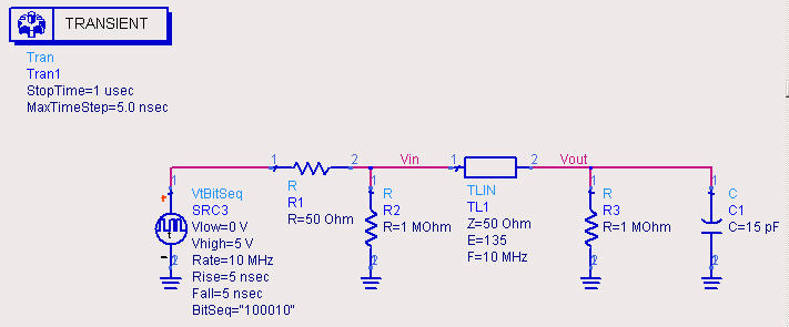
In an ADS schematic, create the following circuit:
You will need the following palettes:
|
Lumped-Components |
Resistors and Capacitor |
|
Sources-Time Domain |
BitSeq Source |
|
TLines-Ideal |
Transmission Line Element |
|
Simulation-Transient |
Transient Simulation Element |
To name the nodes 'Vin' and 'Vout',
press the ![]() button on the toolbar, type in 'Vin' or 'Vout', and click on the
appropriate wire.
button on the toolbar, type in 'Vin' or 'Vout', and click on the
appropriate wire.
Perform the following simulations:
1.
Electrically Short Line: Set E = 10 for the TLIN
element (E is the electrical length in degrees with respect to the entered
frequency - a value of 10 is electrically short, as 360 degrees = one
wavelength) and perform a simulation (![]() button on toolbar). On a display
window create two plots -- one for Vin
and one for Vout as a function of time. Comment on
the results. In specific, what do these results indicate about the necessity of
performing matching for electrically short lines? Include both plots in lab report.
button on toolbar). On a display
window create two plots -- one for Vin
and one for Vout as a function of time. Comment on
the results. In specific, what do these results indicate about the necessity of
performing matching for electrically short lines? Include both plots in lab report.
2. Matched Load: Set R3 = 50 Ohm and E = 135. Perform a simulation with R2 = 1 MOhm and another simulation with R2 = 50 Ohm. Also try changing the electrical length. Does the electrical length matter in this case? Why or why not?
o Include all plots in lab report. (You can select a plot by clicking on it, copy and paste it in Word. Please resize plots to fit about 8 to a page.)
o Answer the above questions.
3. Mismatched Load: Now set R3 = 1 MOhm and R2 = 1 MOhm. Perform simulations for E = 90, 135, 180, and 360. Comment on your observations. Pick out a particularly peculiar case and explain what is happening.
o Include all plots in lab report.
4. Mismatched Driver: Set R2 = 50 Ohm and perform and repeat Step 3.
o Include all plots in lab report.
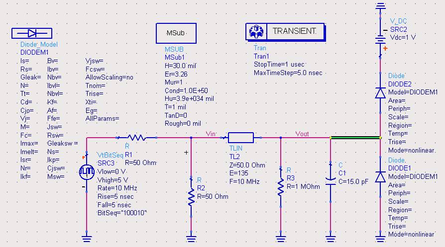
5. Diode Termination: Augment your circuit to look like the following diode clamping circuit. Be careful to verify each of the values. You can either type the name of any new parts (Diode_Model, V_DC, etc.) into the component name field and press enter to place the part or you can add the parts by finding them in their respective palettes. You can get the DC voltage source from the 'Sources-Time Domain' palette and the Diode and Model from the 'Devices-Diode' palette. You should not need to set any parameters on the diode or the model. Simulate this circuit with the highlighted (green) wire connected and disconnected. Specifically compare Vout of the two simulations. What happened to the amplitude of your signal?
o Include all plots in lab report.
o Comment on the behavior of this circuit.
Measurements
1. On the O-scope, switch the terminal impedances of both channels to 1 Megaohm.
Set the generator to produce rectangular pulses with an amplitude of about 200 mV.
- Sketch your observed waveform and observe the amplitude of the O-scope signals as you vary the frequency (don’t worry about plotting any standing waves again, just indicate whether you observed any steady state variations (standing waves) on you transmission line, and which end(s) of the line they were visible from).
- Sketch a circuit equivalent and explain your results in the context of matching in digital systems.
2. Repeat this same procedure including observations and sketches for all possible combinations of channel impedances.
- R2=50 Ohm, R3=1 MOhm
- Sketch your observed waveform and observe the amplitude of the O-scope signals as you vary the frequency.
- Sketch a circuit equivalent and explain your results in the context of matching in digital systems.
- R2=1 MOhm, R3= 50 Ohm
- Sketch your observed waveform and observe the amplitude of the O-scope signals as you vary the frequency.
- Sketch a circuit equivalent and explain your results in the context of matching in digital systems.
- R2=50 Ohm, R3= 50 Ohm
- Sketch your observed waveform and observe the amplitude of the O-scope signals as you vary the frequency.
- Sketch a circuit equivalent and explain your results in the context of matching in digital systems.
Conclusion
Write a summary of what you learned about impedance matching in digital circuits from the laboratory exercises and simulations. Explain what matching conditions are necessary to preserve a digital signal at the output of a transmission line and why.
Again, be sure to follow the
description
of expected lab submissions.
Copyright © 2005 by BYU Electrical Engineering Dept. All rights reserved
Last updated on Feb 4, 2005