Diode
Matched AM Demodulator
Overview
In this laboratory we will use
T-line matching techniques to match to a diode. The diode will be the
demodulation element in a microwave receiver circuit-- essentially, a very
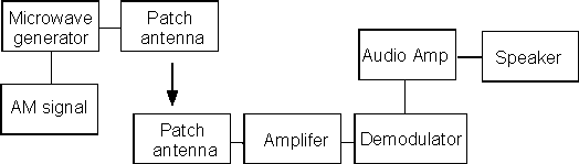
high frequency crystal radio. The following figure shows a block
diagram of the system.
Each group will design the matching network for
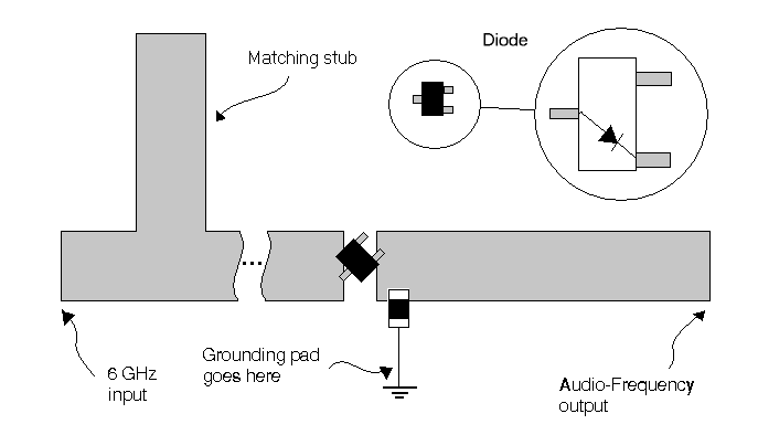
the diode demodulator shown in the figure below and then insert their diode
demodulator into an AM modulated communications system to test its performance.
The not-to-scale figure below shows the basic layout and placement of the diode
and chip capacitor. The diode we will use is the Hewlett Packard HSMS-2850
Surface Mount Zero Bias Schottky Detector Diode. Data 1
and Data
2 contain the data and application sheets.
Procedure
Notice that this system has two
parts that make it a little more complicated than the previous arrangements.
You are to match to a diode rather than a resistor and there is a capacitor
connected to ground. Use the following steps to handle these new issues.
- Calculate the width
of the Microstrip line. This can be done using the LineCalc tool. Use
the following values for your calculations:
- Er = 3.357
- H = 30
mils (substrate thickness)
- Capacitor selection.
The value of the capacitor is chosen so it can be approximated as a short
circuit (~ 1 to 3 ohms) at 6 GHz and an open circuit at audio frequencies
(1-20 kHz). You will be given a chip capacitor for use in your circuit.
Calculate its impedance at the audio and microwave frequencies.
- Diode equivalent
circuit. In order to match the diode impedance you must calculate its
value from the SPICE model equivalent circuit. The equivalent circuit
appears as shown below:
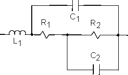
Use the
following values in your impedance calculations: operating frequency of 6 GHz,
L1=2 nH, R1=20 ohms, R2= 9 K ohms, C1=0.08
pF, and C2=0.16 pF.
- Because the capacitor
essentially grounds the 6 GHz signal, you can model the circuit as
shorting at the capacitor for RF frequencies. Although there is some
reactance, the audio end feeds into an audio frequency amplifier, where
the 6 GHz signal will likely find many other capacitive paths to ground.
Circuit Simulation
Using the values determined in the
previous section, create a schematic for your matching network, then run a
simulation on it. Be sure to include the proper gaps for attaching your chip
capacitor and diode. Typically 50 mils is about right. You can look at the
dimensions given on the data sheets (the “Data 1” link at the top
of this page). You can use the LineCalc tool now to solve for the line widths
that will give you the desired characteristic impedances for your transmission
lines. This tool is found in the tools menu and takes the place of the Matlab
script that you developed in earlier labs.
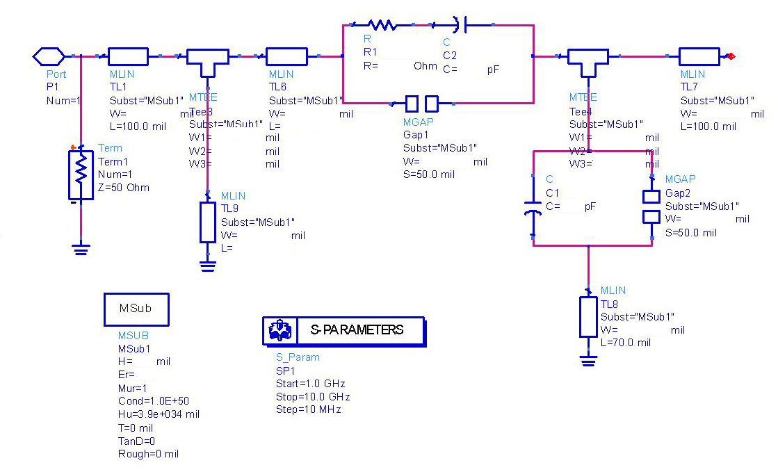
R1 and C2 in this schematic are
the impedance model values for your diode. C1 is your value that you selected
in Procedure section #2. Notice the schematic below uses a shorted stub (TL9)
In this format an open stub is generally more dependable (because you do not
have to drill and solder for the short) and is recommended for this lab.
Layout
Before following the instructions for exporting and milling,
you need to generate the layout first. This can be done by "Layout->Generate/Update
Layout..." You will have to press okay on a couple different
windows to generate the layout. During this process your layout is
automatically minimized, so you will have to maximize it again to see the
results. You may have to readjust some of your transmission lines in the Layout
window to reflect the proper orientation and spacing. Then, follow the
"exporting and milling" instructions as outlined on the lab page.
Send to be Milled
Follow these directions to prepare
and submit your layout for milling.
Exporting
ADS Designs for Milling
Test (2 weeks later)
Retrieve the milled component,
assemble, test and report.
In your lab report explain how you
took your design from simulation to a test circuit and the challenges it
presented. Did your demodulation circuit function properly? How could you tell?
If it did not appear to work, give likely reasons for the faulty circuit. Be
sure to include copies of your calculations, design choices, schematic,
simulation results, and layout in your report.